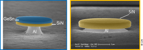
Demonstration of a continuous laser beam with germanium-tin alloy
Researchers from the Centre for nanoscience and nanotechnology (C2N - Université Paris-Saclay, CNRS) have developed a new materials engineering method for manufacturing a germanium-tin (GeSn) alloy laser microdisk, together with researchers from Germany’s Jülich research centre and French-Italian company STMicroelectronics. Using this approach, a continuous laser beam can be observed for the first time with group IV semi-conductor components. It also greatly reduces the operational power requirements compared with the components used up until now.
Semi-conductor lasers are undoubtedly the largest-selling industrial laser and the technology is found in a multitude of everyday applications, including pointers, lasers, CD and DVD readers, laser printers, optical fibres and telecommunications. The majority of these lasers operate with III – V binary components, so called with reference to the columns in which these elements are found in the periodic table devised by Mendeleev. The industrial microelectronic technology in which they are embedded itself uses elements from column IV of the table, such as silicon. This is a marked difference, and one which has its difficulties for larger-scale application of the technology.
Recent work by researchers at the Centre for nanoscience and nanotechnology (C2N – Université Paris-Saclay, CNRS) and the Jülich research centre in Germany, together with STMicroelectronics, is breaking new ground in a laser technology based solely on group IV semiconductor elements. By combining a special germanium-tin alloy (GeSn) with a layer of silicon nitride, they produced a continuous laser beam with the microdisk manufactured. The threshold pumping power densities for this laser beam, i.e. the minimum level of supplied power required for the beam to operate, are sharply reduced (by a factor of 100) compared with the threshold densities for existing GeSn lasers.
Limitations of the current process
The usual technique for obtaining GeSn alloy consists of introducing as much tin as possible – at least 7% – into the germanium. “It involves alloying tin (Sn) atoms into a germanium (Ge) crystal. To create the alloy, atoms must be removed at random from certain points on the pure Ge crystal and replaced with Sn atoms,” explained Moustafa El Kurdi, a researcher at C2N. This creates a compound a direct band alignment structure, making it possible to emit laser light.
There is nothing simple about this manufacturing process, however. The alloy grows on a germanium substrate which, like any crystal, has a specific interatomic distance, known as the “lattice constant”. For the two crystals to create an alloy without any interface defects, the crystal being grown needs to adapt its lattice constant to that of the substrate. When the lattice constants are different, in case of lattice mismatch, the material deposited becomes deformed. Sometimes, these deformations are so great that they result in dislocation, cracking the crystal and impairing the result. In the case of a GeSn alloy growing on a germanium substrate, the extent of the lattice mismatch is such that a very dense dislocation network forms at the interface. Considerable pumping power density is then required to produce the laser beam.

In search of the lattice match
“We explored the hypothesis that increasing the proportion of tin in the alloy would increase the lattice mismatch. We therefore decided to work with a material containing less tin than in the literature, so there were few defects to rectify,” said Moustafa El Kurdi.
The procedure developed by the researchers uses a low percentage of tin in the GeSn alloy, 5.4% instead of the 10% to 16% seen in the literature. Ordinarily, this tin-poor alloy is a very poor emitter owing to its indirect band gap, a configuration which makes laser emission impossible. To produce a laser beam from it, researchers harvested the GeSn crystal after growth on the germanium substrate and turned it over to machine it and remove the region containing the dislocations. They then placed it in contact with a layer of silicon nitride (SiNx). The result is a defect-free layer of GeSn on top of the layer of SiNx, which itself rests on an aluminium base.
“The SiNx is deposited in a series of layers and the final layer deposited only covers the top and sides, like an all-over glaze. The layers of SiNx above and below are under huge stress, just like a tightly coiled spring. When they slacken off, they take the GeSn with them, applying tensile stress which deforms it, pulling on it from all sides. This is the “all-round stressor”, a system that we have patented with STMicroelectronics,” explained Moustafa El Kurdi.
A three-stage system, it involves first treating the defects in the GeSn layer. High tensile stress is then applied to the GeSn to obtain the direct alignment band structure essential for a laser beam. Lastly, the aluminium dissipates the heat that is generated by the device warming up when it is used. Using this system, the GeSn alloy produces a continuous laser beam, with a lasing threshold (the pump power required for it to operate) two orders of magnitude lower than those reported in the literature.
These results pave the way for the manufacture of laser sources based on group IV components, which are much better suited to large-scale industrial use.